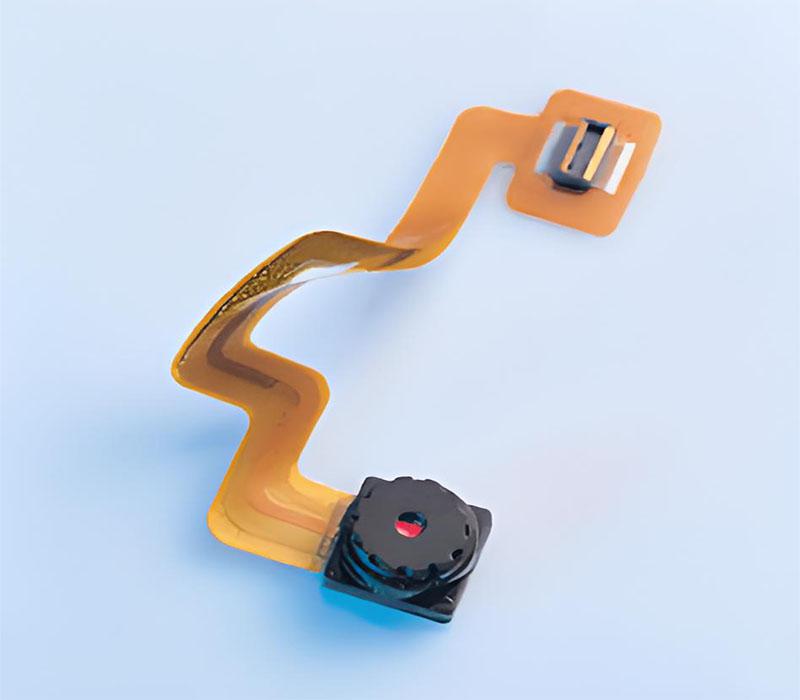
Advanced Multilayer PCB Technical Specifications: Ensuring Precision and Quality

Introduction
Multilayer Printed Circuit Boards (PCBs) are essential components in modern electronics, providing complex interconnections within compact designs. The technical requirements for multilayer PCBs encompass various aspects such as layer registration, dielectric layer thickness, inner conductor thickness, and etching processes. This document details the technical specifications for multilayer PCBs, with a focus on layer registration, dielectric thickness, inner conductor thickness, etching, and negative etching, incorporating Gekunflex brand references to ensure compliance with industry standards.
Layer Registration
ANSI/IPC-ML-950C Requirements
Outer Layer Registration: Measure at least 10 connection pads/holes at extreme positions (e.g., two at each corner and two at the center) to determine the registration between the PCB's outer layers. For connectors without holes, assess the registration by comparing the deviation between the centerline of the reference and the least registered pad.
Inner Layer Registration: Follow IPC-TM-650 method 2.5.16 for electrical testing of custom samples to evaluate layer-to-layer registration.
Compliance: Registration must adhere to specified tolerances, ensuring no violation of design rules or connector tolerances.
Non-Destructive Testing: Use IPC-D-949 designs or supplier-added samples for non-destructive measurement of layer registration.
Destructive Testing: Employ metallographic sectioning of plated holes if dedicated registration samples are not used.
GJB362A-96 Requirements
Unless otherwise specified, layer-to-layer misregistration must not exceed 0.36 mm.
Dielectric Layer Thickness
ANSI/IPC-ML-950C Requirements
The minimum thickness of the dielectric layer must conform to the layout diagram.
GJB362A-96 Requirements
For types 1, 2, and 3 boards, the minimum thickness of bonding sheets and laminates should meet the layout diagram's specifications. Dielectric layers must include at least two bonding sheets or laminates.
After curing, the dielectric thickness between adjacent conductors must be at least 0.09 mm.
Inner Conductor Thickness
ANSI/IPC-ML-950C Requirements
- The thickness of inner conductors must adhere to the layout diagram's specifications.
GJB362A-96 Requirements
- Inner conductor thickness should conform to layout diagram specifications. When copper foil weight requirements are specified, the thickness reduction can be less than 10% of the minimum allowable thickness of the corresponding raw material specification.
Etching or Epoxy Resin Removal
ANSI/IPC-ML-950C Requirements
- If specified, PCBs should be etched before plating to remove resin and/or glass fibers from the inner walls of holes. Etching depth should be between 0.005 mm and 0.08 mm, preferably 0.01 mm. If functional performance is not adversely affected, the etching can be extended up to 0.08 mm. Masking is allowed on one side of each connection pad.
- If etching is not specified but used by the manufacturer, it should be confirmed not to impair the final product. Etching should not exceed 0.03 mm.
GJB362A-96 Requirements
- When specified, etching must remove resin and glass fibers from the inner conductor side of the PCB before hole plating. The minimum etching depth should be 0.05 mm, maximum 0.080 mm, with a preferred depth of 0.013 mm. Copper penetration into glass fibers can extend up to 0.080 mm but must not reduce the distance between conductors in adjacent holes below specified values. Etching should affect both surfaces of each inner conductor. Negative etching is not allowed.
Negative Etching
ANSI/IPC-ML-950C Requirements
- Negative etching is undesirable. If present, it should not exceed 0.08 mm for Level 1, 0.04 mm for Level 2, and 0.13 mm for Level 3 when not specified in the layout diagram.
Conclusion
Multilayer PCB technology is vital for advanced electronic applications, demanding precise adherence to technical specifications. Gekunflex ensures that its products meet stringent standards for layer registration, dielectric thickness, conductor thickness, etching, and negative etching. By following these guidelines, manufacturers can achieve high-quality, reliable PCBs that meet industry requirements and support the advancement of electronic technology.

- Art
- Causes
- Crafts
- Dance
- Drinks
- Film
- Fitness
- Food
- ເກມ
- Gardening
- Health
- ໜ້າຫລັກ
- Literature
- Music
- Networking
- ອື່ນໆ
- Party
- Religion
- Shopping
- Sports
- Theater
- Wellness


